PAPER ● OPEN ACCESSRead More
1. Introduction
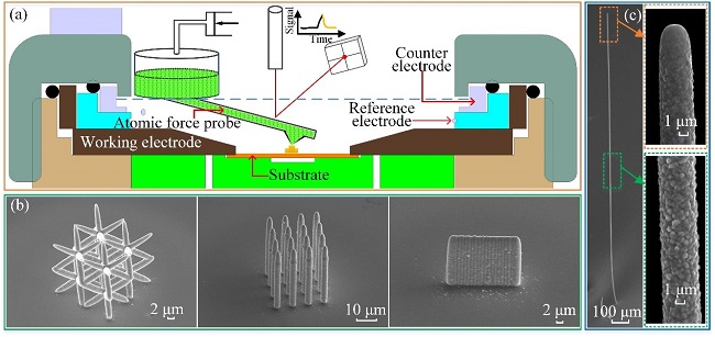
High-quality data transmission, high-precision information sensing, and high-sensitivity signal detection are important means to achieve precise perception and effective identification. High-performance chips, terahertz transmission T/R components, and extreme environment sensor manufacturing technologies have become key frontier research hotspots. Its effective implementation strongly depends on the ultra-precision micro-nano manufacturing level of the complex microstructure of core functional devices. As an excellent carrier for information-enabled core functional devices, pure copper metal has ultra-high electrical conductivity, thermal conductivity and high ductility, as well as low-loss signal transmission capabilities. Therefore, it has received extensive attention in the field of micro-nano manufacturing. Recently, Prof. Huadong Yu, Researcher Jinkai Xu*,Wanfei Ren, Zhongxu Lian, Xiaoqing Sun, Zhenming Xu from Changchun University of Science and Technology wrote an article "Localized Electrodeposition Micro Additive Manufacturing of Pure Copper Microstructures" on IJEM.In this article, the authors have systematically introduced the localized progress of the micro-additive material manufacturing method of the micro pure copper structure, and improves the manufactured microstructure for performance testing. Figure 1 shows the scheme of the LECD-μAM. (a) The three electrodes system in the electrolytic cell. (b) The lattice monomer, pillar array and a thin wall. (c) A high aspect ratio (about 500) wire.
Highlights
● Propose a mathematical model of the synergy of pulsed micro-jet, focusing electric induction and atomic force servo.
● The manufacture of pure copper microstructure is realized, and the deposition rate can reach 0.887μm/s.
● Tested the shear modulus of pure copper microspring, reaching 60.8GPa.
● The Z-direction position of the atomic force probe and the bending state of the cantilever can be detected online at the same time.

Figure 1.Scheme of the LECD-μAM. (a) The three electrodes system in the electrolytic cell. (b) The lattice monomer, pillar array and a thin wall. (c) A high aspect ratio (about 500) wire.
2. Background
The rapid application of pure copper microstructures and devices in the field of 5G communications and highly sensitive detections serves as a driving force for the continuous development of related micromanufacturing technologies. Especially for the signal and data transmission between electrical devices and device units, microstructures have played an irreplaceable role. In the last two decades, major efforts have resulted in the superior manufacturing abilities of microstructures. Recently, two important frontiers of microstructures manufacturing have been the integration of microfabrication and micro additive manufacturing (AM). In microfabrication, although the micromachining resolutions of the two technologies of focused ion beams and electron beam lithography are very high, these methods usually have expensive and difficult to upgrade steps. A technology combining the two methods of micro-milling and micro electrical discharge machining has been proposed for the manufacture of micro-cavity arrays. The size feature obtained with this technique is a few hundred microns. It is technically difficult to apply this technique to micron or even sub-micron accuracy. In micro additive manufacturing, ultraviolet-assisted direct writing technology has been utilized to generate a three-dimensional (3D) independent helical spring-shaped as a strain sensor, but this technology is limited to the manufacture of non-metallic structures. In comparison, direct ink writing (DIW) has overcome the challenge of manufacturing metal structures such as 3D electronic and optoelectronic microstructures, and it has proven to be a useful approach in manufacturing freestanding spiral architectures on flexible and rigid substrates at the scale of tens of micron by further combining laser and DIW technologies. However, such methods still remained limited in fabricating pure metal structures. Additionally, although laser-induced forward transfer and chemical etching for pure metal has proven to be effective methods, the processing quality needs to be further improved. Atomic layer deposition (ALD) can generate microstructure, but the constraints of reactants and deposition conditions limit its usage for a wide range of applications. In addition, focused ion beam induced deposition (FIBID) has been used to grow a 105-nm-diameter carbon spring and a 25-nanometer-thick gold layer deposited on an outer surface. The spring was used to transfer the direction of wave propagation. However, this process cannot achieve the one-step metallization manufacturing of micro springs.
3. Recent Advances
The latest progress is mainly divided into the following two parts: the deposition rate and structural properties, the element composition and mechanical properties of the deposit.
Printing rate and structures performance analysis
Among them, the deposition rate is a parameter that is more important in the micro-additive manufacturing process. Through real-time observation of the deposition state, the Z-axis displacement of the probe and the bending of the cantilever can be measured simultaneously. The results showed that it took 361s to deposit a coil spring with a wire length of 320.11μm, and its deposition rate was 0.887μm/s, and the entire deposition process can be adjusted arbitrarily online by simply changing the extrusion pressure and applied voltage.

Figure 2. Simultaneous measurement of the actual position of the Z axis and the bending of the AFP cantilever. The blue line represents the real-time position of the Z-axis motor in the vertical direction, and the red line represents the cantilever deflection curve of the AFP. In the enlarged view inside, it can be clearly seen that the deposition rate in the gray shading area is significantly higher than the subsequent deposition rate.
Elemental composition and mechanical properties of the deposit:
During the overall deposition process, the tip of the hollow atomic force probe has been immersed under the surface of the supporting solution to avoid the influence of air components on the sediment. The results show that the content of copper in the sediment is greater than 99.5%. When testing the mechanical properties of the micro-coil spring, it showed strong mechanical properties. The shear modulus reached 60.8GPa, which was much higher than that of bulk copper (44.2GPa).

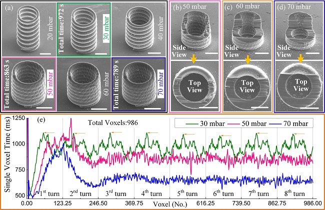
Figure 3. Print information of the deposited sprial springs. The cathode (working electrode) was applied voltage as -0.5 V, the total number of the single 8-turn close-packed spring including 986 voxels for each. (a) The morphological characteristics of the spiral microstructure under different extrusion pressures (20 mbar to 70 mbar with a 10 mbar interval) of the same printed file. (b) The side view and top view of the spiral spring milled by FIB printed in 30 mbar. (c) The side view and top view of the spiral spring milled by FIB printed in 50 mbar. (d) The side view and top view of the spiral spring milled by FIB printed in 70 mbar. (e) The deposition time of a single voxel for the whole printed peirod in extrusion pressure of 30 mbar, 50 mbar and 70 mabr respectively. And the 8-turn was separated by vertical lines clearly. The scale bar is equal to 10 μm in (a)-(d).
4.Perspectives
Although LECD-μAM technology can be used to manufacture pure copper microchip bridges, micro antennas, micro sensors, and other small structures without masks and supporting materials, the technology still has a low deposition rate and is prone to a probe clogging problem. The next step of the research is to introduce a parallel manufacturing method for multiple probes to increase the deposition rate while applying a reverse voltage to avoid probe clogging.
5.About the authors

Professor Huadong Yu, a doctoral supervisor, is a professor of School of Mechanical and Aerospace Engineering of Jilin University, and an adjunct professor of Changchun University of Science and Technology. He is also the chief technology officer of Key Laboratory of Cross-scale Micro-Nano Manufacturing of Ministry of Education, At the same time, he is the chief technology officer of "973" project, and the member of the professional group of control and photoelectric application technology in Central Military Commission Army Weaponry, the overall expert of the National Key R&D Program of "Additive Manufacturing and Laser Manufacturing" of the Ministry of Science and Technology. Simultaneously, he is a member of the Mechanical Teaching Steering Committee of Higher Education Ministry of Education, and deputy of the Teaching Guidance Subcommittee of Mechanical Basic Courses Chairman, Vice Chairman of the Chinese Society for Metrology and Testing, deputy director of the National Technical Committee for Standardization of Optoelectronic Measurements, founding chairman of the International Society of Nano Manipulation Manufacturing and Measurement (3M_NANO), member of the Evaluation Committee of National Higher Education Institutions, deputy director of the Extreme Manufacturing Branch of the Chinese Mechanical Engineering Society.At present, he is mainly engaged in research work in the fields of precision and ultra-precision processing technology, micro-nano manufacturing technology, and micro-opto-electromechanical system technology. He has completed more than 20 provincial and ministerial scientific research projects and obtained 85 authorized invention patents; he has won three provincial and ministerial-level scientific and technological prizes, and two national teaching achievement prizes. At same time, he published more than 60 high-level academic papers and 2 academic works. The developed precision micro-manufacturing system, rapid optical inspection instrument, precision measuring instrument and many other achievements have been applied and promoted, which has promoted the progress of regional scientific and technological level.

Jinkai Xu, researcher and doctoral supervisor, is currently the director of the National and Local Joint Engineering Laboratory of Precision Manufacturing and Detecting Technology/Key Laboratory of Cross-scale Micro-Nano Manufacturing of the Ministry of Education, and the leader of the micro-nano manufacturing discipline of Changchun University of Science and Technology. At the same time he is a young member Ministry of Science and Technology "Additive Manufacturing and Laser Manufacturing" National Key R&D Program General Expert Group, a director of Cutting Advanced Technology Research Branch of China Machinery Industry Metal Cutting Tool Technology Association, and a senior member of China Mechanical Engineering Society, the first committee of the Society of Extreme Manufacturing Branch of China Mechanical Engineering Member. He successively obtained bachelor's, master's and doctoral degrees in engineering from Northeast Forestry University, Changchun University of Science and Technology and Changchun Institute of Optics, Fine Mechanics and Physics, Chinese Academy of Sciences. Undertook more than 20 provincial and ministerial-level projects, and won one first level prize of National Defense Technology Invention Award and one first level prize of Jilin Province Technology Invention Award.He has long been engaged in basic and applied research in the field of cross-scale micro-nano manufacturing, ultra-precision sensing and testing. He has been authorized 35 national invention patents, published 47 SCI/EI academic papers as the first author or corresponding author, and participated in the compilation of an academic work. Department. Independently developed small five-axis ultra-precision processing systems, small laser-assisted processing systems, precision sensing and testing instruments and other equipment, as well as cross-scale micro-nano manufacturing technologies and processes. The research results have been applied to many major projects such as aerospace, lunar exploration, and ordnance industry, which has promoted technological progress in the field of micro-nano manufacturing. The innovation team of "Key Ultra-precision Micro-Nano Manufacturing Technology" led by him was selected as the leading team of young and middle-aged science and technology innovation in Jilin Province. His research has contributed to promoting the regional innovation capability of precision manufacturing equipment and comprehensively improving the development level of the high-end manufacturing equipment industry in Jilin province.


