REVIEW ● OPEN ACCESSRead More
1. Introduction
The growing demand for electronic devices, smart devices, and the Internet of Things constitutes the primary driving force for marching down the path of decreased critical dimension and increased circuit intricacy of integrated circuits. However, as sub-10 nm high-volume manufacturing is becoming the mainstream, there is greater awareness that defects introduced by original equipment manufacturer components impact yield and manufacturing costs. The identification, positioning, and classification of these defects, including random particles and systematic defects, are becoming more and more challenging at the 10 nm node and beyond. Very recently, the combination of conventional optical defect inspection with emerging techniques such as nanophotonics, optical vortices, computational imaging, quantitative phase imaging, and deep learning is giving the field a new possibility. Hence, it is extremely necessary to make a thorough review for disclosing new perspectives and exciting trends, on the foundation of former great reviews in the field of defect inspection methods. Prof. Jinlong Zhu, Dr. Jiamin Liu, Prof. Shiyuan Liu from Huazhong University of Science and Technology, China and Dr. Tianlai Xu, from Harbin Institute of Technology, China, wrote a review " Optical Wafer Defect Inspection at the 10 nm Technology Node and Beyond" on IJEM. In this article, the authors have introduced the research background, systematically discussed the latest progress and the trend of optical wafer defect inspection. This work can be of importance to both new entrants in the field and people who are seeking to use it in interdisciplinary work. Figure 1 shows the Schematic of optical systems that are capable of tackling the diverse challenges in patterned defect inspection.
Highlights
In this article, the authors have presented a comprehensive review of the emerging optical techniques in the past decade with a focus on three specific areas:
(1) the defect detectability evaluation.
(2) the diverse optical inspection systems.
(3) the post-processing algorithms.
This review has disclosed that cutting-edge techniques such as nanophotonics, optical vortices, computational imaging, quantitative phase imaging, and deep learning can make a profound impact on sub-10 nm defect inspection. Because smartphones, tablets, digital televisions, wireless communication infrastructure, network hardware, computers, and electro-medical devices are stimulating the global demand for semiconductor chips, this article may pave new revenues for the field of semiconductor wafer defect inspection.
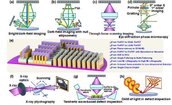
Figure 1. Schematic of optical systems that are capable of tackling the diverse challenges in patterned defect inspection. (a) Brightfield/darkfield imaging system, (b) Dark-field imaging with null ellipsometry, (c) Through-focus scanning imaging microscopy, (d) Epi-diffraction phase microscopy, (e) Patterned wafer containing logic dies and 3D NAND memory dies, (f) X-ray ptychography, (g) THz wave-based defect inspection system, and (h) Coherent Fourier scatterometry techniques using different OAM illumination beams.
2. Background
Growing demand for smartphones, tablets, digital televisions, wireless communication infrastructure, network hardware, computers, and electro-medical devices is stimulating the global demand for semiconductor chips. Moreover, the Internet of Things (IoT) – aka, internet of connected devices – is in its infancy but will contribute significantly to the demand for semiconductor chips in the long term, as will the growth of smart grids, smart cities, and automated smart manufacturing. These imperious demands, together with the endless pursuit of lowering both costs per wafer and energy consumption, constitute the primary driving forces for marching down the path of decreased critical dimension (CD) and increased circuit intricacy. Very recently, Taiwan Semiconductor Manufacturing Company (TSMC) and its Research Alliance partners, announced the 3 nm breakthrough, which offers a path to delivering chips with significant improvements on today's leading 5 nm chips. It’s a big win for fabs and manufacturers all around because it’ll only be two years for 5 nm to have fully settled in the market, but it’s also a nightmare to the entire community of process control, especially for wafer defect inspection: ever-decreasing sizes of features and spaces in these patterns have dramatically strained the capabilities of all the current solutions in balancing the sensitivity, specificity, processing speed, and capture rate. As double patterning, triple patterning, or even quadruple patterning ultraviolet (UV) lithography are now widely used, the number of inspection steps scales up with the increase of patterning steps, which potentially decreases the throughput and increases the risk of device failure because the missed defect detection events will be transferred to the end process. To make things worse, the extremely complex fin field-effect transistor (FinFET) and gate-all-around (GAA) nanowire (NW) devices are now employed to reduce leakage current and improve device’s stability beyond the technology node of 22 nm, which, results in the fact that the key defects of interest in this three-dimensional (3D) architectures are typically sub-surface (especially voids), buried in the stack, or are residues in high aspect ratio structures. Overall, as the industry starts large-scale sub-10 nm high-volume manufacturing, there is greater awareness that defects introduced by original equipment manufacturer components impact yield and manufacturing costs. This grand challenge, undoubtedly, affects the entire semiconductor manufacturing supply chain. Therefore, wafer defect inspection systems have become increasingly important to the fab.
The wafer defect inspection system detects physical defects and pattern defects on wafers and obtains the position coordinates of the defects. Defects can be divided into two categories, i.e., random defects and systematic defects. Random defects are mainly caused by particles that attach to a wafer surface, so their positions cannot be predicted. The major role of wafer defect inspection systems is to detect and locate defects on a wafer. Systematic defects are primarily caused by the variations of the mask and exposure process and will occur in the same position on the circuit pattern of all the projected dies. They occur in locations where the exposure conditions are very difficult and require fine adjustment. Typically, wafer defect inspection systems detect defects by comparing the image of the circuit patterns of the adjacent dies. As a result, systematic defects sometimes cannot be detected using a conventional wafer defect inspection system. Depending on if the inspection is performed on a patterned process wafer or on a bare wafer, wafer defect inspection systems have different configurations. For bare wafers, optical inspection systems, especially the darkfield microscopy, are the workhorse, due to the fact that the primary defects (i.e., particles and scratches on the wafer) have high sensitivity at their high-frequency scattering components. While for patterned wafers, defect inspection is much more complex and challenging due to the complex topography of patterns and various materials on the wafer. Therefore, sophisticated instruments alongside advanced modeling and post-processing algorithms are playing an increasingly important role in patterned wafer defect inspection. In this article, Professor Jinlong Zhu gave a detailed introduction to the recent progresses of optical wafer defect inspection and its most recent progress.
3. Recent Advances
Recent advances in optical wafer defect inspection can be categorized based on the sources of errors, including materials, wafer pattern topography, optical inspection system, and post-processing algorithms.
Effect of Materials on Defect Detectability
Figure 2 presents a preliminary summary of the complex refractive index, the reflectivity under normal incidence R, and the penetration depth δ of the typical bulk materials that are widely used in integrated circuit devices. For the cases where the defects are buried inside the background pattern and the size of patterns is much smaller than the wavelength, the difference in the image contrast between defects and background pattern is then primarily determined by the difference in the optical properties of materials, i.e., refractive index and reflectivity. In other words, the reflectivity contrast between the defect material and the pattern material shown in Fig.1(c) could help in seeking for the optimal inspection spectrum. Therefore, finding an optimal spectrum range in which the image contrast and sensitivity are high enough is more important than improving the optical resolution. This is especially critical at advanced technology nodes.

Figure 2. (a) The refractive index n, (b) the extinction coefficient k, (c) the reflectivity R under normal incidence, and (d) the penetration depth δ=λ/(4πk) as functions of wavelength.
Effect of Topography on Defect Detectability
For patterned wafer inspection, the SNR and image contrast is primarily affected by the sizes and types of defects. Figure 3 presents several typical defects in the periodic Line/Space nanostructure, which is widely seen in the memory devices. The eight subfigures successively present the schematic diagrams of cutting, the horizontal bridge defect at the edge, the intrusion, the zig-zag bridge, the horizontal bridge in the line, the particle, the protrusion, and the perpendicular bridge defect. Up to now, the effects of topography on defect detectability have been widely investigated, which is usually associated with the optimization of defect inspection configurations. For example, both the horizontal and vertical bridging are rather sensitive to the polarization of the illumination beam. With the same defect inspection configuration, different types of defects such as bridge and line cutting present different defect detectability. Certainly, the size of defects and patterns also directly affect defect detectability.

Figure 3. Typical defects in the periodic Line/Space nanostructure on the patterned wafer. (a) Cutting, (b) By bridge 1 and void, (c) Intrusion, (d) Zig-zag bridge, (e) By bridge 2, (f) Particle, (g) Protrusion, and (h) Bx bridge.
Diversity in Optical Inspection Systems
Light is electromagnetic radiation within the portion of the electromagnetic spectrum that is perceived by the human eye or artificial detectors. An arbitrary light field can be fully described by four fundamental quantities, i.e., frequency, amplitude, phase, and polarization. Typically, optical defect inspection is implemented in the regime of linear optics. Therefore, different from amplitude, phase, and polarization, frequency is independent of light-matter interactions. Accordingly, optical inspection systems can be categorized by the measurands of light in practical use. Figure 4 presents one of the inspection systems that is based on the phase reconstruction, i.e., the diffraction phase microscopy and optical pseudo electrodynamics microscopy, in which the perturbated wavefront induced by the defect has been demonstrated that has a very high SNR.
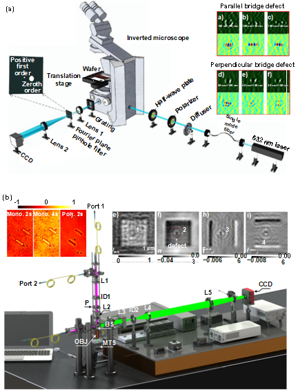
Figure 4. System configurations of (a) epi-DPM and (b) OPEM. The insets on the top right corner of each sub-figure are the measured signals with respect to wafer defects.
Post-Processing Algorithms
From the simplest image difference operator to the complex image synthetic algorithm, the post-processing algorithm plays a critical role in optical defect inspection in terms of improving SNR and contrast of defects. This is especially the case as deep learning algorithms emerge as a ubiquitous part of our daily life. Die-to-die inspection method compares the image of defect-free dies with that of faulty ones to identify the defects in the logic chips, and it was also called the random inspection. Cell-to-cell inspection compares the image of a cell with that of an adjacent cell in the same die to identify the defects in the memory chip, and it was also called the array inspection. Die-to-database inspection uses the differential images, which are obtained by subtracting the image of a target from the modeled image database of the design layout, to identify the systematic defects on the wafer. To identify a defect from a raw image, the key is to ensure the area that contains a defect in the post-processed image (for instance, the differential image) is noticeably larger than a pre-defined threshold. The workflow of deep learning-based defect inspection is quite straightforward, i.e., capture enough e-beam or optical images of wafers (which can be either experimental or simulated ones), train a chosen neural network to extract useful features directly from the images, test the trained model with a small set of samples, and decide if the training should be repeated according to a pre-defined cost function that characterizes the confidence level of neural network. However, deep learning has not been widely accepted in the actual production line, especially for optical inspection. The reasons may not only include the ‘black-box nature’ and lack of interpretability, but also include the unproven capability of positioning and classifying deep-subwavelength defects from pure optical images. To make deep learning techniques applicable in the optical defect inspection in the fab, more works need to be implemented, especially the study of the grey area of deep learning in optical defect inspection and the exploration of the boundary between deep learning and optical physics.
4. Perspectives
From Rayleigh scattering’s point of view, the amplitude of light scattered by any deep subwavelength nanostructure with primary dimension d from a beam of unpolarized light of wavelength λ is proportional to d3/λ2. Therefore, amplitude-based systems are inherently insensitive to deep-subwavelength defects. To boost the SNR and contrast of defects, hyperbolic Bloch modes that are conventionally involved in metamaterials are applied in the detection of buried defects in 3D NAND flash memory. The strong resonance modes induced by the back-and-forth reflection of electromagnetic waves in the Bragg grating-similar cavity play a critical role in the amplification of defect signals. Phase-based defect inspection systems, different from amplitude-based ones, are linearly proportional to the height of defects, which makes phase measurement a potentially high-sensitivity approach for defect inspection. Akin to the orbital angular momentum of light, polarization state nowadays is well-understood as the consequence of spin angular momentum of light. For monochromatic light, the spin and orbital angular momentum densities are the functions of the electromagnetic field and its spatial gradient, which indicates, at least in principle, that the defect sensitivity can be optimized by customizing the illumination light field for a given nanopattern. X-ray ptychography, different from any aforementioned optical defect inspection techniques, is the only optical method that can directly image both surface and undersurface sub-20 nm defects for the entire wafer. As the complexity of both materials and geometry in modern IC keeps increasing, the combination of diverse systems for meeting diverse challenges may be a trend. In conclusion, there may be three potentially important topics relating to optical defect inspection from an academic point of view. The first is the 3D computational imaging of a patterned wafer at very short wavelengths (for example, hard X-ray regime). As a hard X-ray beam is only weakly absorbed by silicon wafers, X-ray ptychography has the potential to penetrate the field by providing revolutionary 3D resolution and sensitivity once the drawbacks including the synchrotron x-ray light source, a massive amount of data, and the low speed being conquered in the future. The second is the structured light field-based inspection mechanism that treats the inspection as an optimization problem for maximizing defect sensitivity. Brightfield, annular, and dipolar illumination modes are widely adopted in conventional defect inspection tools. However, the use of these illumination modes is more like an experience-driven action. A physical connection of the illumination modes and defects is missing. As the surrounding patterns of defects are fundamentally consists of lines and circles, it is possible to customize a structured light field to suppress the background scattering without sacrificing the SNR of defects by exciting the background patterns into dark modes. The last is the sample-oriented inspection, in which the characteristics of samples (such as geometrical structures and optical properties of materials) are pre-investigated for optimizing an optical inspection system. This is also what the industry is doing. Optical defect inspection, though is a long-standing engineering problem, has been regained vitality with the explosive growth of consumer electronic devices and the fusion of emerging techniques such as nanophotonics, structured optical field, computational imaging, quantitative phase imaging, and deep learning. The aforementioned optical inspection systems, though were originally designed for patterned wafer defect inspection, are also critical to many other fields, including but not limited to photonic sensing, biosensing, and turbid photonics.
5. About the Authors

Jinlong Zhu is a full professor at HUST. Jinlong Zhu received his BS degree in Mechanical Engineering from Huazhong university of Science and Technology in 2010, and earned his PhD in Mechatronic Engineering from Huazhong university of Science and Technology in 2015. From 2015 to 2020, he worked as postdoctoral researcher at the University of Illinois at Urbana-Champaign until he started his appointment of Professor with Huazhong University of Science and Technology in 2020. He conducts research in basic science and engineering at the intersection of optical physics, nanodevices, semiconductor IC chips in industrial robots, and machine learning. He is particularly interested in the application of tools, knowledge and insights from photonics, electronics and nanoscience to the design of advanced Photoelectronic measurement systems for the noninvasive exploration of nanoworld.

Shiyuan Liu is a Professor of Mechanical Engineering at Huazhong University of Science and Technology, leading the Nanoscale and Optical Metrology Group with research interest in metrology and instrumentation for nanomanufacturing. He also actively works in the area of optical lithography, including partially coherent imaging theory, optical proximity correction, source mask optimization, and inverse lithography technology. Prof. Liu received his PhD in mechanical engineering from Huazhong University of Science and Technology in 1998. He holds 42 patents and has authored or co-authored more than 150 peer-reviewed technical papers.

Jiamin Liu, received a Ph.D. in Mechanical Engineering from Huazhong University of Science and Technology in 2020, and is currently a postdoctoral researcher in the Department of Instrument Science and Technology, Huazhong University of Science and Technology. He is mainly engaged in the research of ultrafast dynamic polarization measurement technology and instruments, high temperature and high pressure Mueller matrix ellipsometry measurement technology and instrument development, nanostructure defect detection theory and equipment development, etc. He has published more than 10 SCI papers and applied for 16 invention patents.

Tianlai Xu, Associate Professor,the member of the Space Intelligence Committee , Chinese Society of Space Research. He received bachelor's, master's and doctor's degrees in engineering from Harbin Institute of Technology. The main research interests include aircraft dynamics and control, autonomous navigation, target detection and data fusion. He was responsible for one project of National Natural Science Foundation of China and participated in a number of 973 and 863 projects. He has published more than ten academic papers and authorized 8 invention patents.


